
After last week's post I set myself three more tasks to get done:
- Get some decent fault handling setup
- Get the onboard LEDs working
- Try running code from the SDRAM
I've managed to achieve all of them, but they weren't all as easy as I'd thought.
Fault handling
Last time I was working on the SDRAM and was hitting some issues which ended up with a hard-fault. It's hard to diagnose these faults efficiently without a bit of diagnostic code. There are actually a group of hardware exceptions which can occur in the Cortex-M processor, if the exceptions aren't enabled then they all get handled as hard-faults. The exceptions that can occur are:
- Hard fault - something went badly wrong like a vector table load failed or another fault handler did something wrong.
- MemManage fault - a memory access violation, usually related to the Memory Protection Unit (MPU) but there are some hard coded restrictions that can trigger this
- Bus fault - accessing an area of the memory map that isn't connected to anything for example
- Usage fault - invalid instruction, usually means you're trying to execute something that isn't code like a data table or GPIO register
Each of these faults can trigger an exception like an interrupt, jumping execution to the address in the vector table. They each have further details available about the cause of the fault to help diagnose the problem. I had a set of fault handlers pre-made which I've used before. They dump the relevant information about the fault onto the serial port as easy to read text. I had to customise the code slightly to match it up to my hardware (the console is on UART3 on this board but the code was written for a Cortex-M4 with console on UART1). The code is in one C file check it out on GitHub. Mostly this approach is based on the excellent book The Definitive Guide To the ARM Cortex-M3 by Joseph Yiu (now covers M4 as well but my copy is older than that!).
Using my code with CubeMX requires you to disable the CubeMX exception handlers because you need the processor to jump straight to my assembly code handler so it can gather the relevant stack and frame info without any C compiler stack manipulation. In CubeMX you can go to the System Core->NVIC (NVIC1 for the M7 in the dual core chip I'm using). In the second pane down you can select the "Code generation" tab and untick "Generate IRQ handler" for each of the four fault handlers.
With the fault handlers in place all I need to do now is wait for me to make a mistake! I always try and get this code in early in a project, the sooner it's in place the more time it saves!
LED driver
This is the bit I expected to be easiest. (Last time I tried to integrate the fault handlers the option to not generate the functions in CubeMX wasn't there so it caused endless removing code from the generated files). It turned out to be a bit challenging.
The LEDs are driven by the MCP23S17 SPI GPIO chip which controls the expansion bus. There weren't any free pins on the STM32 itself to drive them. So I needed to get comms with the expansion bus controller working. This should be a fairly straight forward job, it's just like the GPIO registers of the trusty old 8-bit PIC microcontrollers that I used to use. Firstly I made the mistake of leaving the reset pin in its default (asserted) state which meant the chip didn't work at all. Secondly I found comms were really flaky, the first commands mostly worked but then the next update to change the LED pattern would fail.
This seemed like an electrical issue so I broke out the trusty old TDS210 oscilloscope and started probing. Everything looked fine, the usual suspects like chip select framing ending early or swapped COPI and CIPO lines all checked out. Then I noticed that the LEDs were updating every time when I had a 'scope probe on the serial clock line. It happened every time 'scope on or off, add the capacitance of the probe to the clock line and it works reliably.
Essentially the issue is the long and winding path of the SPI SCK line around the circuit board. This path takes in not only the expansion controller but the slots, including the power supply slot as well as going all the way down to the WiFi module.
The SPI clock signal is being driven at 7.5MHz which whilst slow by modern standards is a fair speed to start thinking of this like a transmission line. I also suspect that the length of the trace and the likely capacitance of it could be picking up significant signal from the 100MHz clock applied to the DRAM. I experimented with various drive settings on the clock line and different values of the termination resistor I'd included in the clock line, with no success. In the end the simplest solution I found was to add a parallel termination of 10k pulling down the clock line so that it is not left floating for its full length. Perhaps this will not be necessary once the WiFi chip is in place at the end of the line.
Executing from DRAM
The last task was to experiment with executing code from the SDRAM. I wanted to see what would happen if I tried to execute code from the default address of the SDRAM which is listed as "Execute never" in the reference manual. Executing code from different locations means linking it at a different address which can be done by modifying the linker file. The even trickier bit about executing from RAM is that the code must be copied there from somewhere after the system boots since RAM is volatile.
I wrote a really simple function to run from the SDRAM, it prints some messages and adds two numbers together. Just adding the two numbers together wasn't enough to make an actual function; the compiler optimised it out.
1 2 3 4 5 6 | |
To make this function appear at a different location in memory I added a decorated prototype just above it which sets a custom section attribute:
1 | |
That line tells the linker to put the compiled code for that function into a section called .sdram1, now the linker script needs to be modified to describe this region. In the linker file I added the two SDRAM regions:
1 2 3 4 5 6 7 8 9 10 11 12 | |
I can access SDRAM1 at either 0xC0000000 or 0x70000000 with the default mapping.
Then I added a section to the file after the .data section:
1 2 3 4 5 6 7 8 9 10 | |
This defines a number of new symbols, _sisdram1 will be a variable with the address of the start of the functions in the .sdram1 section in Flash. That's the source for copying them. _ssdram1 gives the start address in RAM where the functions are designed to be run from. and finally _esdram1 is the end of the functions in RAM so by comparing with _ssdram1 we can tell how much memory to copy from Flash to RAM.
Using those symbols I wrote a copy function that I could use after the initial memory checks are complete to copy the code into RAM:
1 2 3 4 5 6 7 8 9 | |
Because I used uint32_t variables for the addresses the size calculated is in multiples of the size of a uint32_t variable so I multiplied the size by sizeof(uint32_t) in memcpy. I could have used uint8_t variables instead since their size is 1 byte.
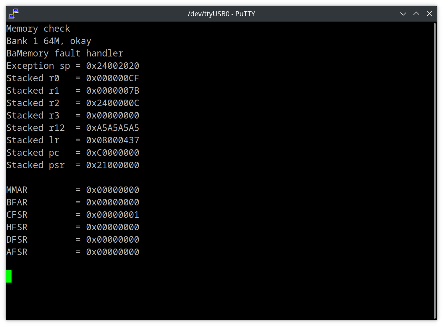
Putting it all together I was able to copy the code then try to call it. I did 3 tests to see how it worked. Accessing the SDRAM at the default address of 0xC0000000, I could copy the functions to it without issue but as soon as I tried to execute from that address I got a MemManage fault.
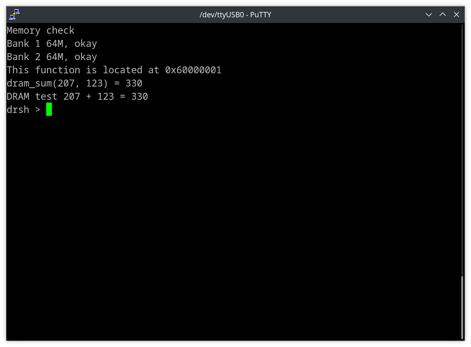
Just tweaking the linker script shown above to change the SDRAM1 region ORIGIN to 0x70000000 was enough to make it all work, the call was now to a section of memory where execution is allowed. I also tried changing the mapping strategy in CubeMX which remapped the SDRAM1 bank to 0x60000000 so I could potentially execute code from bank 1 and bank 2 since they are both in the executable region of memory. Sure enough updating the linker script (and in that case updating the memcheck code as well because the SDRAM banks are no longer mapped at 0xC0000000 and 0xD0000000) it all worked.
Summary
I'm really pleased with this progress. I've achieved all the things I wanted to this week and everything is going the way I expected. Don't be fooled I would have had the memory remapping stuff working twice as quickly if I'd not forgotten to plug the USB to serial cable into the board, I spent ages trying to debug that. Even experienced engineers can still trip up on the simple things. Next I'm going to start on one of the SD card slots and see if I can get SDIO working.