
With a working serial interface it was time to try bringing up the external memory. I've maxed out the available external memory on this chip, it can support up to 64MB of SDRAM on each of the two banks and that's what I've got. To hit the full 64MB capacity you have to have a 16M x 32 memory arrangement. If you only use 16 bit wide memory you get stuck at 32MB because of the number of address lines. I couldn't find any 16M x 32 RAM chips in easy to hand solder packages but 16M x 16 are cheap and plentiful. I drew out the schematic with 4 of these, 2 in each SDRAM bank and shared all the address chip select and control lines between each pair wiring one chip up as D0-D15 and the other as D16-D31. This should work transparently since all the configuration commands sent to SDRAM chips are sent on the address lines which are shared by all the chips so they will all get configured with the same CAS latency, burst length etc.
Software
Setting up the software to configure the SDRAMs was a little tricky. I've done SDRAM before so I'm pretty familiar with the STM32 FMC peripheral but I've never used both banks and I've never done 32 bit data before. Getting it all setup in CubeMX was a mix of guesswork and looking at past projects. Some of the timing settings I can figure out from the datasheet for the memory chips but the definitions of what the ST chip is expecting is a little lacking. The first few tries I couldn't get a clock generated at all until I realised that "SDRAM common clock" which defaults to "disabled" disables the clock output altogether. Perhaps that makes sense for power consumption reasons but I don't understand why you'd configure the peripheral but not generate any output. Once I'd figured that out I set the clock for the FMC peripheral to 200MHz in the clock tree and the SDRAM common clock to 2 HCLK clock cycles. That should mean we're running at 100MHz which means we'll be in PC100 compatible mode. We could go faster with the memory chips I've got but I'll stick with this until something is working.
I had to re-read the section in the STM32 datasheet about calculating the refresh period register and set that up. Then I used the code I had in the article I mentioned above to configure the SDRAM chips. I had to tweak it so it configured both banks instead of just bank 2 like the Discovery board has.
I wrote a really simple memcheck type utility, it scans the 64MB memory space and writes the address to each 32 bit chunk. After that it reads each 32 bit address and compares the contents with the address. If the data matches the contents of memory the RAM must be working. It's always a good idea to write lots of addresses then read back rather than write one then read it back. If you just do one write then one read you can find valid memory just using the bus-capacitance to store the last written value long enough for you to turn around and read it back!
Memcheck fails
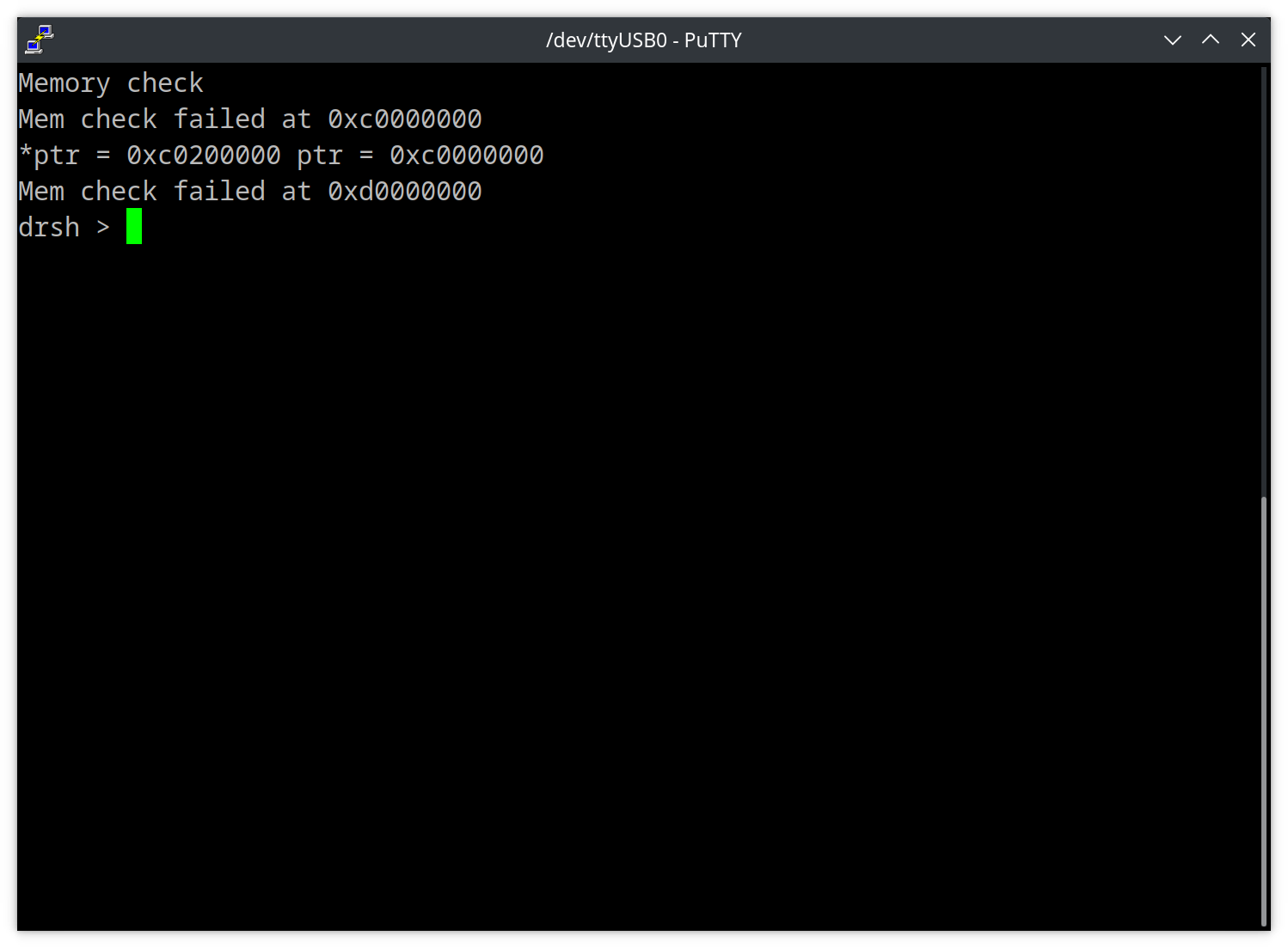
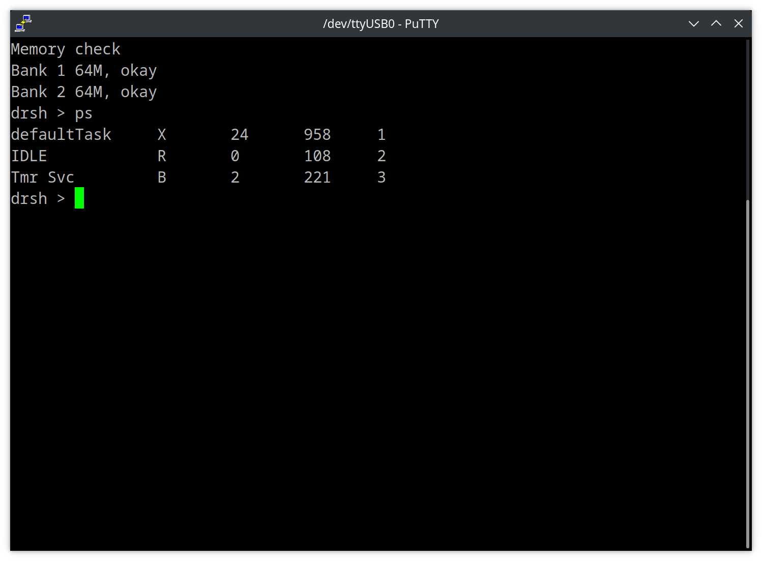
My memcheck code failed on both banks at the very first address read back. That meant it had successfully written all the addresses, so at least the SDRAM was configured correctly. I printed out the failed 32 bit value and noticed that there was a spurious 1 at bit 21. Checking the schematic that pin is on the corner of the chip next to a 3.3V pin. I got out the magnifier and sure enough there was a tiny bead of solder across the two pins holding D21 permanently high.
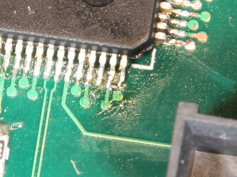
A little dab with the soldering iron and a bit more inspection and it was all cleaned up. I now have 128MB of RAM working on my board!
Now I've proven my memory design I have a few more things to address,
- I want to add fault handlers. The Cortex-M7 has a few different fault handlers which can give useful information about different failures, at the moment these are all disabled which makes all failures call the Hard Fault handler. I've got some code for presenting more useful information from crashes on the serial console which helps with debugging.
- I soldered up the GPIO expander and the 5 LEDs while I was soldering up the RAM. I want to get the LEDs working to help with test and debug.
- I need to look at remapping the SDRAM. There are a few options for where in the memory map the SDRAM appears. So far I've left it at its default position, but according to the datasheet I can't execute code from that address. It looks like there is a remap which will let me execute code directly from the SDRAM which gives much more flexibility for loading code.